Translated into English by Patricia Lima Carlos.
PLLs or Phase Locked Loop are found in AM, FM, modems, frequency synthesizers, wireless phones, cell phones, digital and analog instruments, and in an infinity of other applications where there are frequencies. PLL works with frequencies in the same way that an operating amplifier works with voltages, there is their importance in modern electronics.
Basic PLL
To understand how a PLL works we will analyze its operation in parts, starting with a very simple configuration that is shown in Figure 1.
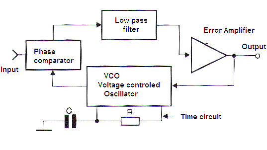
In this circuit we have a block (which we will analyze later) whose output voltage depends on the phase difference between two signals of the same frequency applied to its input.
This voltage is filtered by a low-pass filter which in the simplest configurations is nothing more than a resistor and a capacitor. The signal from this filter works to control the frequency of the final block consisting of a VCO (Voltage Controlled Oscillator). This circuit generates a signal whose frequency can be shifted within a range of values ??from the voltage applied at its input. The signal from this oscillator, as shown in the basic diagram, is applied to the input through a feedback loop.
From the situation where there is no input signal, the frequency of the signal at the output is determined only by the characteristics of the VCO and will be at a central value. If we apply at the input of this circuit a frequency signal f, the phase detector will come into action and compare the frequency of this signal with the frequency of the VCO that is applied to the input.
Assuming the signals have different frequencies, the phase detector will generate A signal that is the difference of the frequencies (f - fo) which will be applied to the filter. The result is, as this frequency is relatively low, when applied to the filter a voltage is created which oscillates sensitively acting on the VCO.
The reaction of the VCO to this ripple applied from the VCO is a frequency change that precisely tends to make its output approximate the frequency from the input signal. As soon as the frequencies equalize, the ripple disappears and the voltage at the output of the low-pass filter stabilizes by "locking" the VCO precisely at the input frequency. We say that the VCO captured the signal or "locked" the signal by recognizing its frequency. In Figure 2 we show in a graph what happens.
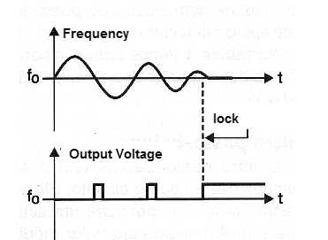
Any change in frequency of the input signal that occurs will generate a new difference signal at the output of the phase detector and a voltage change at the output of the filter that will cause the VCO to "search" for the new frequency.
In theory, a circuit like this would be fairly simple to implement, but would probably not perform as expected for several factors that should be taken into account. Thus, for implementation of a real PLL, we need to go beyond analyzing some important points of its functioning.
Lock Range
Taking the blocks of Figure 1 as an example, we consider that the frequency difference between the input and the generated signal by the VCO was relatively low so that its difference could pass through the second block which is the low-pass filter. If we work with very different signals, the difference may be a frequency too high to pass through the filter and the system does not work. We will not have an output voltage to act on the VCO.
This means that there is a well-defined range of frequencies around which the VCO operates in the circuit can act, locking. This frequency range is called the "lock range".
The lock range of a PLL is given by the difference between the highest frequency and the lowest frequency around fo (center frequency of the VCO) which can be captured, as shown in Figure 3.
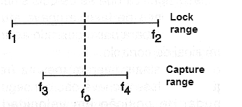
In the common PLLs, which we can obtain in the form of integrated circuits the center frequency fo, can be selected through external capacitors and resistors while the lock range depends on the type.
Thus, for example, an IC such as NE567 can operate with a fo of up to 500 kHz, capturing signals whose frequency range around fo becomes up to 10 to 1, i.e., f1 is 10 times smaller than f2 In the graph of Figure 3.
Phase Detectors
We find two different types of phase detectors in common PLLs. These detectors are called type I and type II.
a) Type I phase detector
The type I phase detector consists of a four quadrant multiplier. To better understand how this type of circuit works, let's imagine that at its input two digital signals of the same frequency are applied, but with a certain phase difference, as we will explain in Figure 4.
Let us imagine that these signals are applied to an O-Exclusive port, which leads us to obtain an output that is formed by pulses whose width corresponds precisely to the phase difference between the two signals. These pulses, according to their width, represent an average voltage which will be precisely proportional to this phase difference as shown in curve (b) of Figure 4.
A very interesting point that we can observe by analyzing this figure is that the frequency of the output signal is the double of the frequency of the input signals (as we will see, this feature allows PLLs to be used to multiply frequencies). The major problem with this type of circuit is that it tends to brake when multiple frequency signals are applied to the input, as shown in Figure 5.
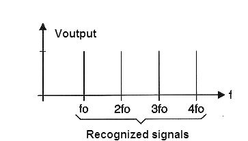
In other words, this type of phase detector is not able to differentiate a signal of the fundamental frequency from a harmonic, and can lock in either one. Another problem that must also be considered is that if the signals applied at the input do not have an active duty cycle of about 50% the type I detector will not work properly. The great positive factor in the operation of this type of circuit is its incoming noise immunity.
b) Type II phase detector
This type of circuit works with the signal fronts applied at the input. In other words, it takes into account the instant the signals change levels which means they must work with rectangular signals. We can compare this detector to a 1-pole x 3-position switch, as shown in Figure 6.
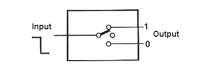
When the input signal has a negative transition, the switch is moved to the logical level 1 position (up) unless it is already in this position. Likewise, a negative transition of the VCO signal makes the circuit switch to 0 logic level (down). This means that the two signals have a phase difference, the key acts up and down thus generating a control signal.
If the signals have the same frequency and phase the switch can not change positions at enough speed and thus takes on an average position where the level is neither high nor low (open circuit).
Note that in this type of detector if the signals are in phase there is no output signal and thus there is no residual signal when it locks. It should also be noted that for the low-pass filter the switch acts as a capacitor charging and discharging the circuit. The filter in this type of detector acts similarly to a sample and hold circuit. Another important point of this circuit is that the lock range does not depend on the low-pass filter.
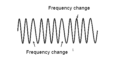
The negative point of this type of phase detector is that it can be deceived by noise in the signal. A signal having oscillations, as shown in Figure 7, may cause the circuit to generate several inapropriate transitions. Noise-free signals should be used with PLLs which have this type of phase detector.
In the table given below we have a performance comparison of the two types of detector:
| Type I | Type II | |
| Active Cycle of the Input Signal | Should be close to 50% | Irrelevant |
| Harmonic Sensitive | Yes | No |
| Noise Sensitive | No | Yes |
| Ripple | High | Low |
| Lock Range | Narrow | Wide |
| Phase difference when the signal is captured | 90 degrees | 0 degrees |
| Frequency when it is “out” of capture | Center VCO frequency | Minimum VCO frequency |
Low-Pass Filter
The Low-Pass Filter has two functions in this type of circuit. It provides a signal which is a voltage whose average value corresponds to the phase difference of the signals and at the same time it determines the speed at which the frequency of the VCO changes.
Since the speed at which it acts on the VCO is an important factor in determining the immunity to the noise present in the input signal, in PLL projects the components associated with the filter must be chosen with the utmost care.
The simplest type of filter is the one formed by an RC circuit, as shown in Figure 8 in (a). However, since this simpler configuration does not guarantee the best performance, a slightly more complex configuration is used, which is shown in the same figure in (b).
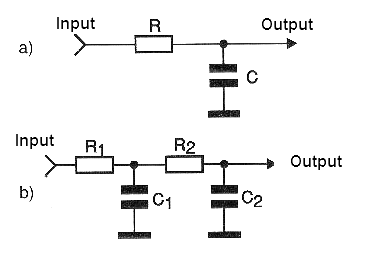
For greater stability the R2 value should be on the order of 1/5 of the R1 value in this type of filter. This rule is only an approximation because there are calculation methods which can be applied in cases where is desired a performance much closer to the ideal one.
Using PLLs
The properties of the circuit being analyzed work as an infinity of practical applications involving the need to recognize a given frequency signal as the starting point for the application. Let's look at some of these applications:
a) Signal Regeneration
There are applications in which it is required that the signal applied to the input of the circuit is exactly the same as that of the output. This type of behavior is especially highly desirable in a modem where it needs to recover signals that travel long distances over telephone lines which deform them.
The designers of digital circuits know that when we increase the signal-to-noise ratio, at the same time we have a decrease of the passband. In the specific case of PLLs the passband is basically determined by the characteristics of the filter. In Figure 9 we show how it is possible to implement demodulator for FSK signals using a PLL.
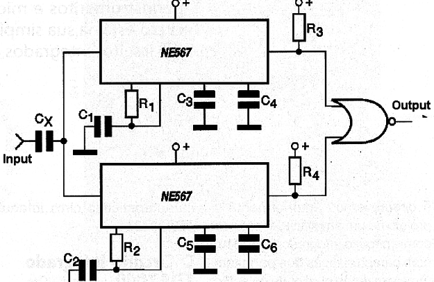
Of course, data transmissions using FSK are no longer used, but the circuit works as an example of application.
b) FM Demodulation
This is a very interesting function that can be implemented using a PLL. This type of application for PLLs in particular is used in communication circuits because they are much more linear than relational or quadrature detectors.
However, the circuit is also somewhat more expensive because of the need to have a linear VCO and to be able to operate at much higher frequencies. In this type of application, the VCO is connected in such a way that its center frequency is the same as the intermediate frequency used in the receiver with which it operates.
The lock range must be at least twice as wide as the frequency range in which the signal is shifted when modulated in frequency, as shown in Figure 10.
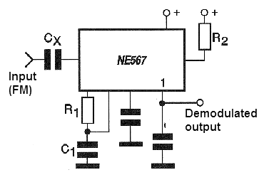
For example, for a common FM receiver having a FI of 10.7 MHz and a modulation bandwidth of 75 kHz these are the values ??to be considered in the design, as shown in Figure 10. Another similar application is the shown in blocks in Figure 11.
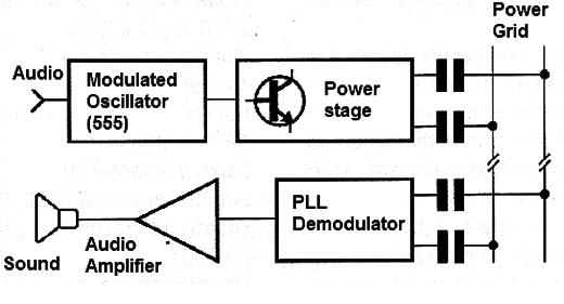
The signal from an audio amplifier frequency modulates a high frequency oscillator. This modulated signal in frequency is applied to the power grid being separated by a high-pass filter at the input of the remote receiver.
This signal is applied to the PLL which then demodulates it for amplification by an audio amplifier. This is the working principle of many office intercoms and electronic nannies.
Conclusion
PLLs are used in a multitude of applications and what we have given was a simple description of its operating principle and some applications in practical circuits. There are many integrated circuits of PLLs like the 4046, NE567 and others that can be used in projects whose frequencies reach up to a few megahertz.
Special types can be found for applications at higher frequencies, but their operation and mode of use does not change. By analyzing the datasheets of such components readers can now have much easier understanding of their features and how to use them in a new project.


