We explain what Bandgap or BG means, a term for Forbidden Band, better known in our technical terminology.
Let's start with the properties of atoms of materials commonly used in electricity and electronics when they are isolated. We begin by analyzing the atoms individually.
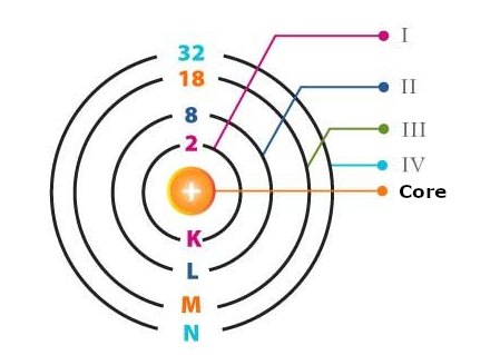
As we know, electrons revolve around atoms in well-established orbits or layers representing different energy levels, as shown in Figure 1.
To these layers, we can associate energy levels that depend on the material. As we can see in Figure 2, energy levels are measured in electron-Volts or eV.
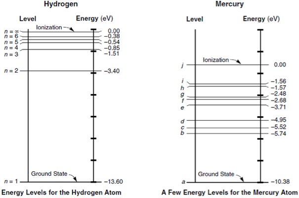
Note that the closer to the core, the higher the energy level. When it reaches zero, the electron can break off from the atom. Ionization takes place.
Note that there are gaps in which electrons cannot stay among the allowable energy levels of the various layers. There is, therefore, a bandgap in which no electrons can exist.
When the atoms in the material form a crystalline structure, an interaction takes place between them. Electrons from one atom are shared with an adjacent one, but in such a way that the energy levels are slightly different.
As a result of this phenomenon, we expand the forbidden band or bandgap towards the outermost electrons, the valence electrons.
But, the important thing for electronics is that this expansion of the forbidden band occurs in different ways, thus determining the electrical nature of the material. It determines whether the material will be a conductor, a semiconductor, or an insulator.
The variation in the dimensions of the forbidden region is not sudden, determining a transition between conductors and insulators. It is continuous and not only valid for pure materials formed by materials of a single type. It is valid for alloys, thus enabling semiconductor materials doped with different elements to have other electrical properties.
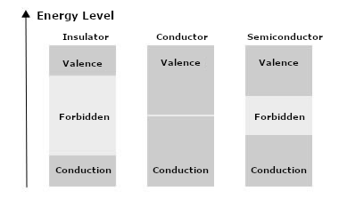
We need to know that there are then two regions in which electrons can stay. The conduction band, where electrons can be released and move, originating an electric current or ionization, and a valence band.
Many electrons can cross the forbidden band at room temperature and enter the conduction band, thus making the material conductive. As this band is tiny in conducting materials, this explains why they have so many electrons available to drive an electric current.
In silicon, the energy required for the electron to cross the forbidden band is 1.1 eV and for germanium 0.67 eV. Germanium, therefore, has a higher number of charge carriers available than silicon. Note that for insulators, the forbidden band is much more significant.
When we add impurities to the material, the forbidden band changes, giving the materials different properties regarding conduction. Likewise, alloys of two materials also have other properties.
We know that the addition of impurities changes energy levels and, therefore, the way electrons can move, giving rise to extrinsic materials of the N and P types, which are vital for electronic devices.
The result is that electron donor and acceptor materials in semiconductor materials cause the forbidden band to change.
WBG and UWBG
With common semiconductor materials such as silicon, germanium and eventually others, we have bandgaps or forbidden bands that endow the components formed by joints of those materials with properties well known to all designers.
Germanium junctions need at least 0.2V to conduct, and for silicon junctions, something around 0.7V.
But, new semiconductor materials are being created, enabling the rise of new generations of semiconductor components.
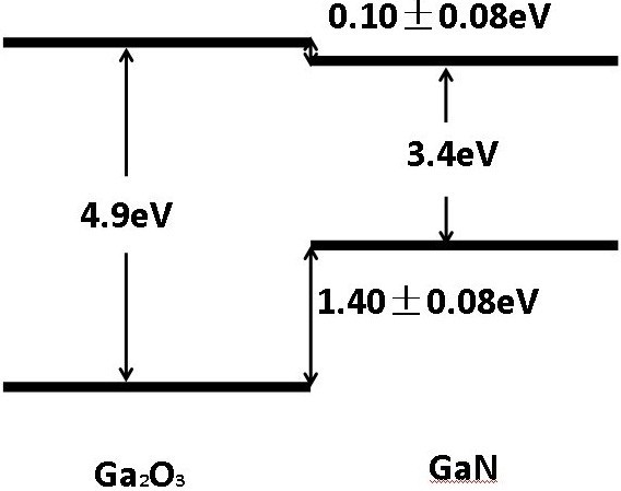
The recent generation of semiconductors with wider forbidden bands, such as SiC (Silicon Carbide), with 3.3 V band, and GaN (Gallium Nitride) with 3.4 V band, in addition to others, such as Zinc Oxide or Diamond, allow the elaboration of much smaller and more efficient power components than the previous equivalents. In Figure 4, the forbidden bandwidth of such materials.
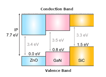
These components are called Forbidden Broadband or Wide Bandgap, abbreviated WBG.
SiC switching transistors are already familiar, with a wide variety of power types available, as we've covered in several suggested components on the website (enter SiC in the website search).
But we can further improve semiconductor performance by using materials with even wider band gaps. These are Ultra-Wide Bandgap or UWBG semiconductors.
Materials with forbidden bands higher than 4 eV are classified as UWBG semiconductors.
In current research in this group, we have materials such as Gallium Oxide (Ga2O3), Cubic Boron Nitride (c-BN) and Gallium Aluminum Nitride (AlGaN).
Figure 5 shows how we can obtain with Gallium a wider forbidden band in the composition with Oxygen, thus creating a UWBG semiconductor.
Benefits
The characteristics of WBG semiconductors allow them to be used with advantages in many applications.
For example, they enable greater efficiency in energy conversion, which is essential in the case of power semiconductors. Ohmic losses are smaller.
They can operate at higher voltages and have a better operating frequency range between 1 kHz and 1 MHz. Operation at higher voltages is because reverse breakdown voltage increases with higher forbidden bandwidth.
Depending on the material used, such as Gallium, ultra-wide bandgap semiconductors also have higher performance with RF signals.
We can say that UWBG components will represent the next generation of power semiconductors, indicating that we still have a long way to go in solid-state electronics before, as many claims, quantum devices become practical.


